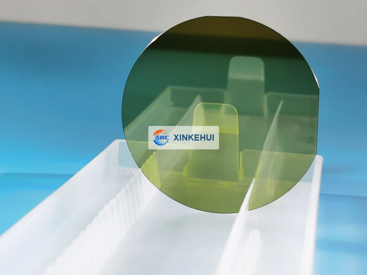
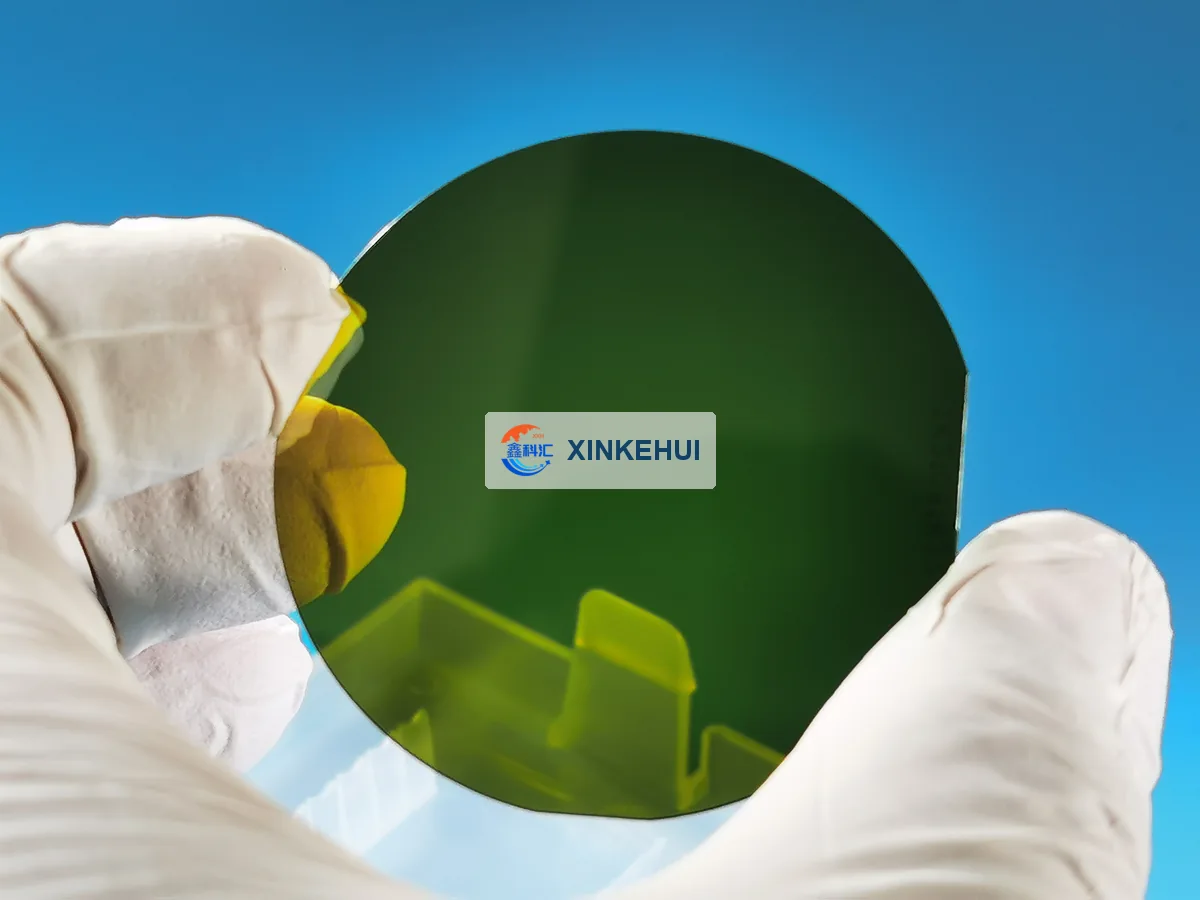
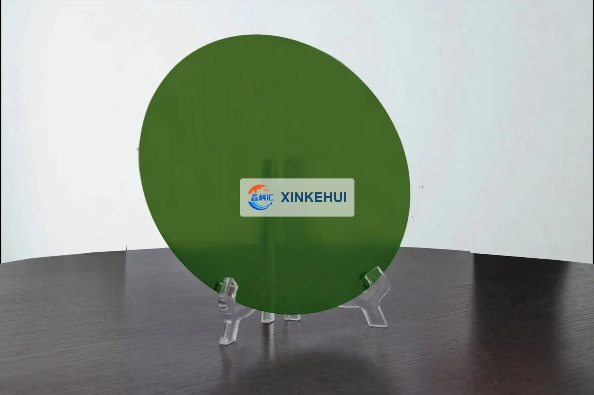
What is a 4H-N SiC wafer?
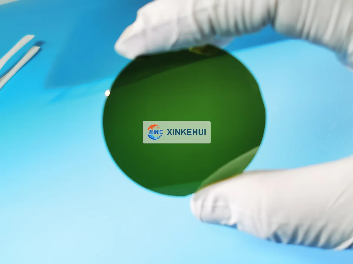
A 4H-N SiC wafer is a nitrogen-doped, N-type single crystal silicon carbide substrate with the 4H hexagonal polytype. It provides a conductive base for appropriate SiC epitaxial structures and power-device manufacturing processes.
Which SiC wafer diameters are listed?
The company profile lists 2, 3, 4, 6 and 8 inch SiC wafers, corresponding to nominal diameters of 50.8, 76.2, 100, 150 and 200 mm. The public overview lists 4H-N SiC across 2–8 inches. Current availability must be confirmed.
What is the difference between N-type and semi-insulating SiC?
N-type SiC substrates are conductive and are commonly used for vertical power-device platforms. Semi-insulating SiC substrates have much higher resistivity and are used where electrical isolation is needed, including GaN-on-SiC RF structures. These materials are not interchangeable.
Are SiC wafers supplied with an epitaxial layer?
The main specification table describes SiC substrates, not a defined epitaxial stack. The public overview separately mentions 4–6 inch SiC epitaxial wafers. For epitaxy enquiries, specify layer thickness, doping, uniformity and defects so the team can review the requirement.
What resistivity is published for 150 mm 4H-N SiC?
The public 6 inch conductive SiC listing gives a resistivity of 0.015–0.028 Ω·cm with nitrogen doping. This value is not a universal specification for all SiC wafers and must not be applied to semi-insulating SiC substrates.
Why is a 4° off-axis orientation used?
An off-axis SiC surface is used in many epitaxial processes to support controlled step-flow growth. The public 150 mm 4H-N listing specifies 4° toward [11-20] ± 0.5°. Confirm the surface face, direction and tolerance against your epitaxy process.
What do CMP and MP mean for SiC wafers?
CMP means chemical mechanical polishing; MP means mechanical polishing. They describe different surface preparation routes. For an epi-ready SiC substrate, agree the target face, roughness, surface damage criteria and cleaning condition rather than relying on the polishing label alone.
How do production, research and dummy grades differ?
SiC wafer grades address different acceptance criteria and intended uses. Production-grade SiC requires process-specific electrical, geometric, surface and crystal-defect limits. Research grade is selected for the experiment; dummy grade is intended for tool or handling evaluation, not automatically device fabrication.
Which crystal defects should a SiC wafer enquiry cover?
Depending on your process, request limits and available measurements for micropipe density, basal plane dislocations, threading screw dislocations, polytype inclusions and surface defects. The portfolio MPD reference is below 1 cm−2, but grade-specific limits must be agreed in writing.
Can SiC wafer thickness or edge geometry be customized?
The company profile indicates customized thickness and lists bevel or C-shape edge options. Supply a drawing with SiC wafer diameter, thickness, tolerance, flat or notch, orientation and edge criteria. Manufacturing feasibility and pricing need technical review.
Are SiC single crystals and seed wafers offered?
The company literature lists 2–6 inch SiC ingots and wafers in conductive and semi-insulating types. Seed-wafer grade is also listed. Specify polytype, conductivity, face, orientation, diameter, thickness and crystal-defect requirements for confirmation.
What inspection documents should I request?
Request the available lot-specific inspection report and agree the required measurements before ordering SiC wafers. Possible items include dimensions, TTV, warp, roughness, orientation, resistivity and defect data. The document scope is subject to confirmation, not assumed for every grade.
What are the price range, stock status and delivery time?
No verified public price range or real-time stock record is supplied for these SiC wafers. Price and lead time depend on diameter, grade, quantity, surface finish and acceptance limits. Request a written quotation and inventory confirmation; this page does not promise immediate availability.
How should SiC wafers be stored and handled?
Keep SiC wafers in their specified protective packaging in a clean, dry environment. Use suitable clean gloves and wafer handling tools, avoid touching polished surfaces and follow your facility’s contamination-control procedure. Confirm the supplier’s packaging and cleaning instructions for the ordered lot.

 CORE MATERIAL